Reverse Engineering a Digital Answering Machine (part 1)
Part 1. Hardware Hookup and Bit-Level SPI
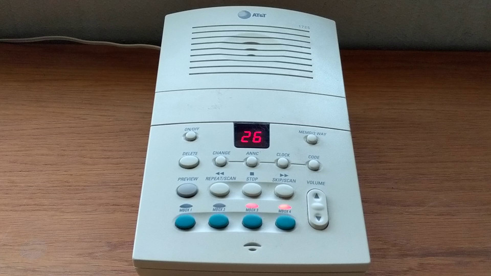
I used this answering machine while I was in college in the early 2000s. When I moved out, I packed it up with the last messages intact and forgot about it. Now back out of storage almost 20 years later, the machine itself doesn’t “spark joy” but it has become a time capsule of voice recordings that I want to archive digitally.
I could connect the analog signal to line-in on my computer or simply hold a mic up to the speaker, but it would be even better to copy the messages in their original digital form. Getting at that source data takes a little reverse engineering.
Anatomy of a Digital Answering Machine
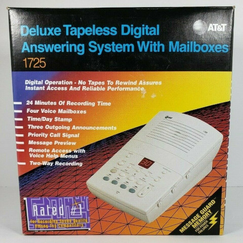
This is the AT&T Lucent 1725 Deluxe Tapeless Digital Answering System with Mailboxes. It’s voicemail for a telephone land line from before mobile phones became common.
Amusingly, these are still listed for over $100 in the year 2020.
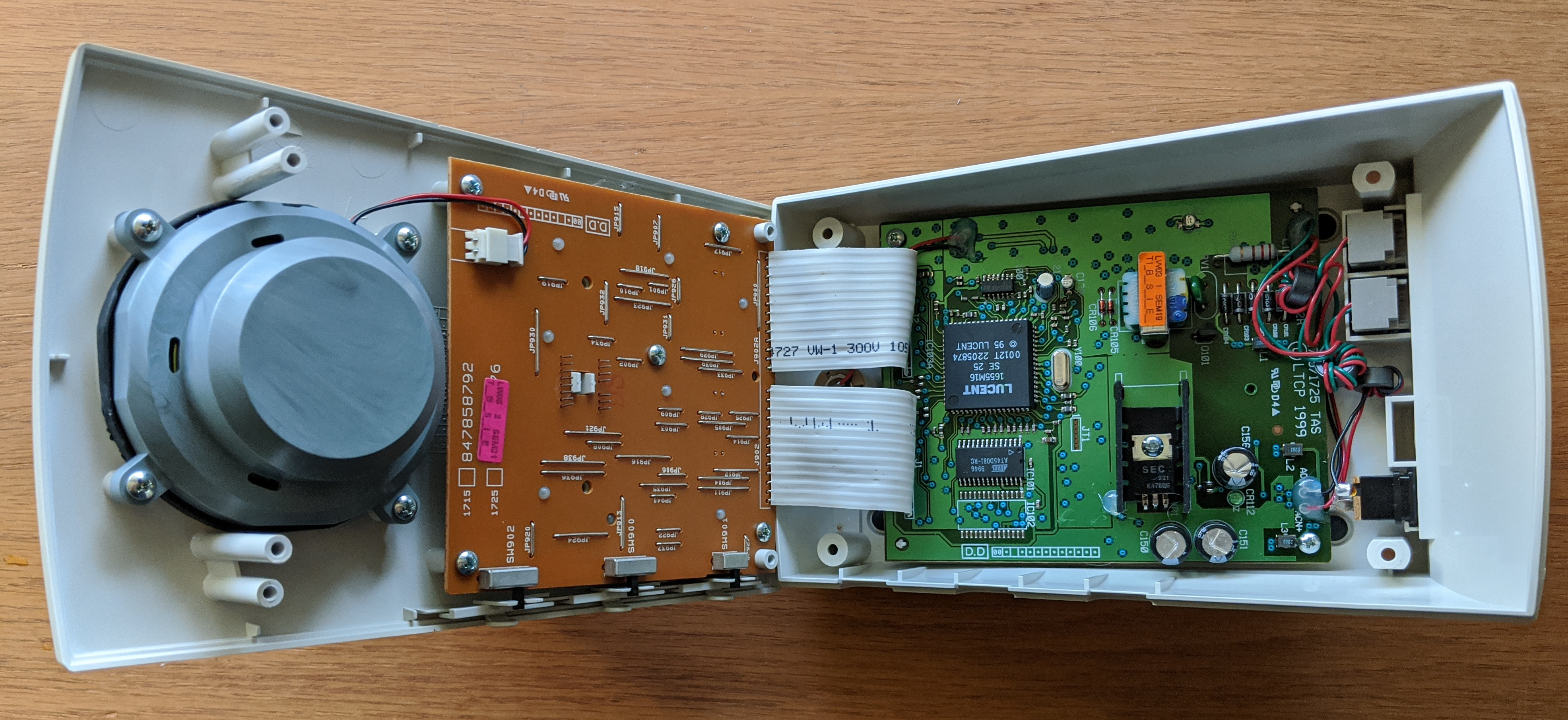
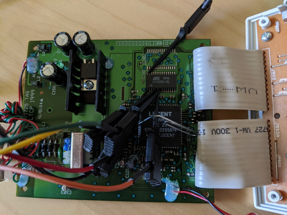
Inside there’s a user interface board and a logic board. The user interface board has all the front panel buttons, LEDs, switches, and speaker. The logic board has 3 chips
-
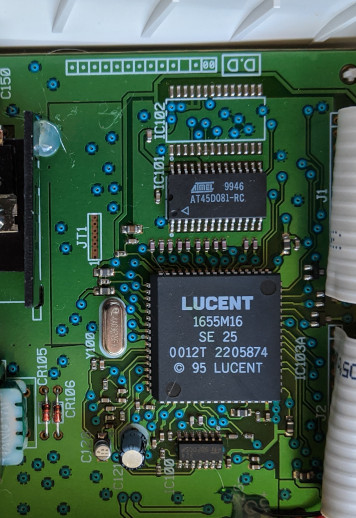
Lucent 1655M16 - I couldn’t find a datasheet for this chip, but judging by the number 1655, it is probably based on the Lucent DSP1600. A writeup in EETimes from 1999 mentions these as a new way to make digital telephone answering machines where the chip functions as both a DSP and microcontroller. “M16” might mean that it is programmed with a mask ROM specifically for this application.
-
ST Micro LM 324 - Op amps for handling analog audio from telephone, speaker, mic.
-
Atmel AT45D081-RC - Atmel DataFlash. A reprogrammable flash chip which is probably where the messages are stored. There’s an unpopulated footprint for an additional chip, maybe to support different flash densities or store more messages in a different model.
SPI Monitoring
The flash chip interfaces over an SPI-compatible protocol where the master sends a command, then the flash chip responds. So to monitor the signals between the controller and flash chip, I connected my USB logic analyzer to the appropriate pins, with a readout in PulseView.
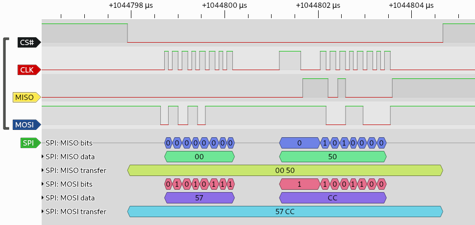
Here’s the first SPI exchange when the machine powers up. It looks like the controller sent 0x57 and the flash responded 0x50. The full-duplex 0x00 and 0xCC are ignored during the command and response.
According to the datasheet, 0x57 is a status register read operation. The flash chip returns a byte in the following format, compared to the 0x50 response shown in the logic trace.
| Bit 7 | Bit 6 | Bit 5 | Bit 4 | Bit 3 | Bit 2 | Bit 1 | Bit 0 | |
|---|---|---|---|---|---|---|---|---|
| format | RDY/BUSY# | COMP | 1 | 0 | 0 | X | X | X |
0x50 |
0 | 1 | 0 | 1 | 0 | 0 | 0 | 0 |
Even before going into detail about what RDY and COMP mean, we can orient ourselves using the middle bits 5, 4, and 3. These indicate the density of the flash chip and are hard coded to 1 0 0 in this model. But bits 5, 4, 3, of 0x50 don’t match 1 0 0. What’s going on?
There are a couple things in the logic trace that I wasn’t expecting to see. What is that extra wide clock pulse in the middle between 8 command bits and 8 response bits? Why does the SPI readout end with a mysterious blank spot on the last clock pulse? It looks like the response bits are shifted.
Skipping a bit on the wide pulse would shift the response bits to the left and bring bits 5, 4, 3 into alignment with 1 0 0. The shifted response of 0xA0 looks more like what we’re expecting in the status register.
| Bit 7 | Bit 6 | Bit 5 | Bit 4 | Bit 3 | Bit 2 | Bit 1 | Bit 0 | |
|---|---|---|---|---|---|---|---|---|
| format | RDY/BUSY# | COMP | 1 | 0 | 0 | X | X | X |
0xA0 |
1 | 0 | 1 | 0 | 0 | 0 | 0 | 0 |
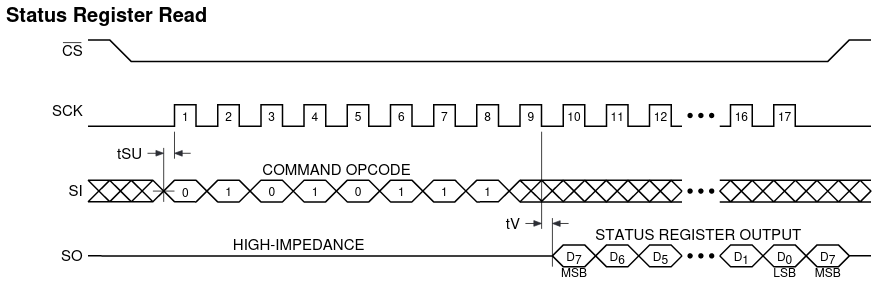
It turns out that the flash datasheet does show this skipped bit (clock 9) in its timing diagram, so the Lucent controller probably inserts that “wide pulse” to skip a bit before reading. PulseView on the other hand isn’t built to handle it because it would need to parse the command set for this specific chip in order to know when the lagging response starts (commands vary in length between 1-8 bytes).
This will come up later when we set up tooling to issue commands directly to the flash chip.
Interfacing With the DataFlash Chip
The interface I’ll be using between my computer and the SPI bus is a BusPirate. The BusPirate (3.3v) can match the voltage of the flash chip (5v) by connecting its built-in pull-up resistors to the target board’s 5v supply.
Under normal operation, the Lucent controller chip is the SPI master, so just connecting the Bus Pirate to the running system won’t work. Both masters would be in conflict trying to drive the SPI lines. What we need is for the Lucent controller to leave its pins in HiZ while the BusPirate talks to the flash chip.
The Lucent controller probably has a RESET# pin, but without the datasheet, it’s difficult to spot. On the other hand, there is a pretty obvious clock crystal with visible traces connecting it to the chip. So I shorted out the clock signal with a paper clip and can power the board without the controller booting up.
By the way, this didn’t work on the first try. While circuit bending the machine, I accidentally got it to delete all messages. Luckily I had analog backups, and it was also possible to undelete them using the bootup SPI trace I captured earlier. More on that later.
With this setup we can dump the chip, do some static analysis and get an idea of how the data is organized in Part 2.